All categories
Featured selections
Trade Assurance
Buyer Central
Help Center
Get the app
Become a supplier


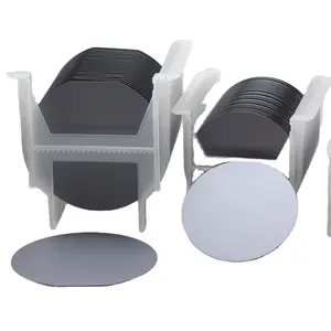


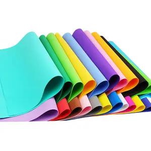
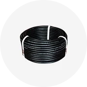
. tấm silicon điện trở suất cao tại Alibaba.com có nhiều loại và đa dạng. Nhu cầu cá nhân của bạn và ứng dụng của. Bạn có thể dễ dàng hài lòng tấm silicon điện trở suất cao tại đây với mức giá tuyệt vời nhất. Không độc hại, chịu điện, bền và chịu nhiệt. tấm silicon điện trở suất cao có thể được tìm thấy ở đây để đáp ứng yêu cầu của bạn. Chất liệu này vượt trội hơn nhiều so với cao su thông thường, truyền thống.
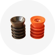
. tấm silicon điện trở suất cao là hỗn hợp silicone với các phân tử khác .. tấm silicon điện trở suất cao ở thể lỏng, rắn hoặc RTV. Mỗi loại trong số này chuyên về các ứng dụng nhất định .. tấm silicon điện trở suất cao là vật liệu linh hoạt, hiệu suất cao và rất độc đáo về bản chất. Do tính tiện dụng cao, bạn cần chắc chắn rằng nó là loại vật liệu phù hợp với bạn.
Alibaba.com tập hợp những người bán. tấm silicon điện trở suất cao từ khắp nơi trên thế giới. Tìm yêu cầu của bạn về. tấm silicon điện trở suất cao, với thông số kỹ thuật chính xác của bạn trong vòng vài phút bằng cách lọc xuống và tìm kiếm qua hộp tìm kiếm dễ sử dụng. Duyệt qua các phiếu mua hàng được xếp hạng bởi những khách hàng trước đây và được thông báo đầy đủ về bản chất của việc mua hàng của bạn. tấm silicon điện trở suất cao trước khi bạn đặt hàng. Liên hệ trực tiếp với người bán và nhận thông tin trực tiếp về sản phẩm.
Nếu bạn chọn từ mảng. tấm silicon điện trở suất cao tại Alibaba.com, bạn đưa ra quyết định cao hơn sẽ hiển thị ngay từ khi bạn đặt hàng. Ứng dụng của bạn sẽ vượt trội về trải nghiệm cho dù là ứng dụng trong lĩnh vực giải trí, chăm sóc sức khỏe, điện tử, thuốc men, ô tô hay sản phẩm tiêu dùng. An toàn và bền, vật liệu này là một trong đó. Các nhà cung cấp và người bán buôn của tấm silicon điện trở suất cao có thể tự hào tiếp thị.