


1Set Traffic Light Signal HO OO Scale LED Model Architecture Train Railroad Crossing Walk Street + PCB Circuit Board
Ready to Ship
$2.52
Min Order: 100 pieces
Shipping per piece: $0.61

In an age where connectivity is key, businesses are constantly seeking ways to enhance signal strength and clarity. Signal booster PCB boards stand at the forefront of this quest, offering a critical solution for amplifying and maintaining the integrity of various signals. This ultimate guide delves into the intricate world of signal booster PCBs, providing a comprehensive look at how to select the right board for your business needs. From understanding the technical nuances of PCB design to exploring the vast array of options available on Alibaba.com, this article is your go-to resource for making an informed decision on signal booster PCBs that will take your business's connectivity to the next level.
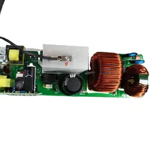
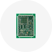
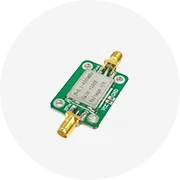
Signal booster PCB boards are integral components in enhancing audio or Wi-Fi signals by amplifying the input signal they receive. The layout of these PCBs is crucial as it can significantly influence the output quality. Issues such as leak resistances, voltage drops, and parasitic capacitance can arise from a poorly executed PCB layout, affecting the amplifier's performance. The design of a signal booster PCB involves a detailed graphic representation of copper tracks on the board, which is meticulously crafted by PCB designers to ensure that the amplified signal is clear and strong.
The functionality of signal booster PCBs extends beyond mere amplification; they are pivotal in converting analog signals into digital formats. Before digital analysis, signals are first amplified, which is essential for applications that require high input saturation to transform analog signals into square waves. This process utilizes harmonic saturation to achieve the desired waveform. Moreover, signal booster PCBs are designed to maintain signal frequency while providing a high voltage output with minimal resistance, enabling them to power devices like loudspeakers effectively.
In the context of PCB design, it's important to consider the placement of components such as bypass transistors and decoupling capacitors. These elements are strategically positioned to meet instantaneous switching current demands and to mitigate voltage noise, ensuring a stable power supply. Additionally, the grounding strategy is critical, with all ground pins needing to be closely connected to the ground plane to facilitate a proper current return path and to prevent the formation of ground loops.
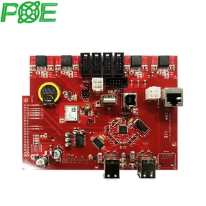
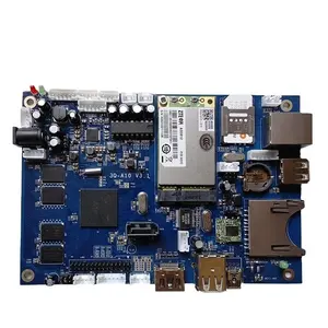
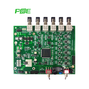
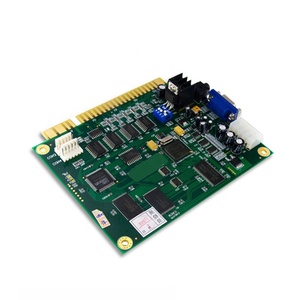
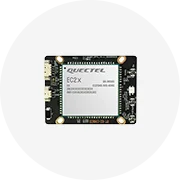
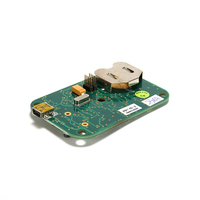
Alibaba.com hosts a diverse range of signal booster PCB boards designed to cater to various signal amplification needs. Among the offerings, you can find multilayer PCBs, which are favored for their enhanced performance and compact size. These boards are typically constructed using FR4 material, known for its dielectric strength and thermal resistance, making it suitable for robust signal booster applications. Additionally, options include 4-layer PCBs that provide more space for circuitry, which is essential for more complex signal boosting tasks.
For specialized applications, Alibaba.com lists PCBs with specific features such as immersion silver for improved conductivity and durability. This is particularly useful in signal boosters where consistent performance is critical. There are also PCBs tailored for wireless applications, including those for wireless microphones, indicating a focus on the telecommunications sector. The platform also showcases PCBs for various other applications, such as Bluetooth audio receivers, indicating the versatility of the signal booster PCBs available.
Furthermore, the site includes PCBs designed for efficiency in power-sensitive devices, like quick charge power banks, and those for use in medical devices, which underscores the reliability and safety standards of the PCBs on offer. For businesses looking for customization, there are services for reverse engineering and PCB cloning, which can be crucial for creating bespoke solutions or replacing obsolete parts. This variety underscores Alibaba.com's role as a comprehensive source for signal booster PCB boards that can meet the needs of diverse industries.

When selecting a signal booster PCB, it's crucial to consider amplifiers' specifications, as they directly impact the board's performance. Key specifications include bandwidth, which should match the frequency range of interest for your application. Amplifiers are categorized into classes, each with distinct characteristics suitable for different applications.
For signal booster PCBs, power amplifiers are often used. These are typically Class B, C, or AB and are designed to operate near their nonlinear compression point. A stable power amplifier should exhibit minimal power output decrease, less than 1 dB, across its operating temperature range.
The nonlinearity of power amplifiers can lead to harmonic distortion, which is undesirable. For audio applications, total harmonic distortion (THD) or total harmonic distortion plus noise (THD+N) are critical metrics, with lower percentages indicating better performance. In frequency modulated signals, third-order intercept point (3OIP) is a specification to watch, as it indicates the level at which third-order intermodulation products reach the same output intensity as the desired signal.
Considering these specifications will guide you in choosing the right signal booster PCB for your needs. While the inherent nonlinearity in amplifiers can lead to effects like harmonic distortion or intermodulation products, understanding and selecting the appropriate specifications can mitigate these issues and ensure efficient operation of your signal booster PCB.
The performance of signal booster PCBs is significantly influenced by the materials used in their construction. Key to this is the substrate's permittivity or dielectric constant (Dk), which affects the size of the amplifier circuits; materials with higher Dk values lead to smaller circuits, beneficial for portable and miniaturized designs. However, for high-power applications, larger circuitry may be necessary for adequate power dissipation.
Consistency of the dielectric constant across the PCB substrate is crucial for maintaining tightly controlled impedances, essential for the impedance matching of power transistors in amplifiers. Moreover, the stability of the dielectric constant with temperature changes is vital, as variations can impact amplifier performance. Materials with a low thermal coefficient of dielectric constant are preferred for their minimal change in Dk with temperature fluctuations.
Another critical factor is the dissipation factor or loss tangent, indicating the signal energy lost through the dielectric material. Lower values are desirable to minimize loss in output power and signal gain. Additionally, moisture absorption by the substrate can significantly alter the dielectric constant, impacting impedance and amplifier gain, hence materials with low moisture absorption rates are advantageous.
Lastly, the material's ability to manage heat through thermal conductivity and a low coefficient of thermal expansion (CTE) is essential, especially for high-power amplifiers where heat dissipation is critical for reliability. Materials with higher thermal conductivity and lower CTE values are better suited to withstand the thermal stresses associated with power amplifiers.
Signal booster PCBs are integral to enhancing communication technologies across various industries. These boards are pivotal in wireless communication systems, where they support the infrastructure that enables mobile and land wired communications. Their applications extend to telephonic and mobile phone tower systems, ensuring robust signal transmission and reception. In the realm of business, PBX systems benefit from the reliability and efficiency of these PCBs, as do industrial wireless communication technologies.
The versatility of signal booster PCBs is evident in their use in video conferencing technologies, which demand high-speed and stable connections. They are also employed in the rigorous environments of space communication technology, where reliability is paramount. The role of these PCBs in cell transmission, tower electronics, and high-speed servers and routers underlines their importance in maintaining the backbone of digital communication infrastructures.
Moreover, signal booster PCBs are found in electronic data storage devices, satellite systems, and video collaboration systems, highlighting their widespread utility. They are also crucial in digital and analog broadcasting systems and VoIP technologies, where signal integrity can significantly impact performance. Lastly, these PCBs enhance security technology and information communication systems, ensuring secure and uninterrupted communication channels across various platforms.
For successful installation of a signal booster PCB, an external antenna placement is crucial, ideally elevated 20 feet up to ensure optimal signal reception. The antenna should connect to the PCB via a shielded cable to a filter that only allows the desired frequency range. Amplification is achieved through a Low Noise Amplifier (LNA) followed by a Variable Gain Amplifier (VGA), which is microprocessor-controlled to prevent signal overload. Proper spacing or shielding between internal and external antennas is necessary to avoid feedback loops.
Maintenance involves manual adjustments using a slide potentiometer to control the VGA, ensuring the amplified signal is within safe operating parameters. Regular testing with a spectrum analyzer or a Software Defined Radio (SDR) can monitor performance, with adjustments made to the VGA gain as needed. The device's proximity to the internal antenna is critical, with a recommended range of about 3 meters to prevent feedback and ensure compliance with transmission regulations.
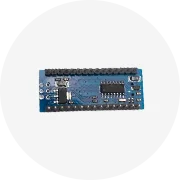
Long-term testing is advised to confirm the durability of the components. The signal booster's design, currently large and complex, aims for future simplification into a single Arduino shield, facilitating easier installation and maintenance. Users are encouraged to verify local telecom regulations before setup to ensure compliance and avoid potential damage to nearby devices during initial testing phases.
Looking ahead in the realm of signal booster PCB technology, several innovations are set to redefine the landscape. Additive manufacturing, or 3D printing, is at the forefront, enabling the creation of complex circuits and uniquely shaped boards, catering to the demand for more customized electronic products. The rise of flexible electronics, utilizing pliable materials, introduces circuit boards that can bend and flex, which could enhance durability and reduce space constraints in various applications. The integration of Internet of Things (IoT) capabilities is becoming crucial as IoT devices proliferate, necessitating PCBs that support low power consumption and wireless connectivity.
Moreover, the application of Artificial Intelligence (AI) in the assembly process is poised to streamline efficiency and minimize errors by analyzing production data. This integration of AI can lead to smarter manufacturing processes and a significant reduction in waste. As signal booster PCBs evolve, these technological advancements will likely lead to increased customization, improved efficiency, and a greater emphasis on sustainability, ensuring that the circuit boards of the future not only boost signals but also align with the evolving needs of technology and consumers.
Selecting the right signal booster PCB is a pivotal decision for any business looking to enhance its communication infrastructure. Throughout this guide, we've explored the intricacies of PCB design, the diverse types available on Alibaba.com, and the key features to consider during selection. We've also examined the impact of materials on performance, the wide-ranging applications across industries, and the future trends that are shaping PCB technology. With these insights, businesses can make informed choices, ensuring their signal boosters are not only effective but also aligned with the latest advancements and regulatory standards. As technology continues to evolve, staying ahead in the realm of signal booster PCBs will be crucial for maintaining robust and reliable communication channels in an increasingly connected world.


 浙公网安备 33010002000092号
 浙B2-20120091-4