Popular in your industry


Related Searches:


Top categories


About n type silicon wafer
Understanding N Type Silicon Wafers
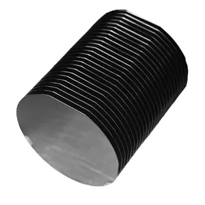
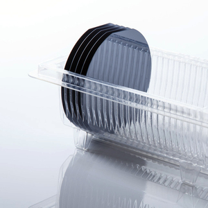
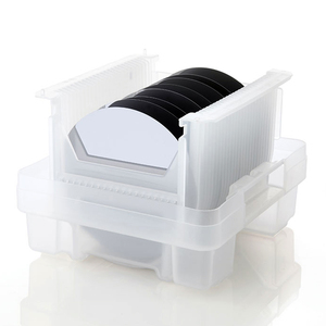
Semiconductors form the backbone of contemporary electronics, with n type silicon wafers playing a pivotal role. These wafers are crafted from silicon, imbued with specific impurities to enhance their electrical conductivity. The 'n type' designation refers to the addition of elements that contribute free electrons, thereby creating a negative charge carrier prevalence.
Characteristics and Applications
The n type silicon wafer is distinguished by its tailored electrical properties, which make it indispensable in the fabrication of various electronic devices. Its primary function is to facilitate controlled electrical conductivity, a fundamental aspect of transistors, diodes, and power devices. These wafers are integral to the production of components that manage power distribution, signal processing, and energy conversion in countless electronic systems.
Technical Specifications
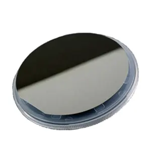
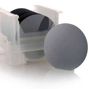
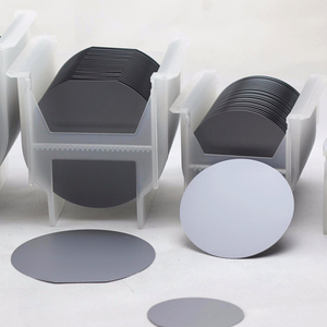
Each n type silicon wafer comes with unique specifications, including size, temperature tolerance, and current output capacity. Their versatility allows them to be utilized in specialized roles, such as in circuits with variable resistance or in applications that require photo-sensitivity. The adaptability of these wafers is further enhanced by their availability in various resistivities and conductivities, catering to a broad spectrum of technological requirements.
Manufacturing and Customization
The production of n type silicon wafers involves a precise doping process, where silicon is infused with pentavalent impurities to achieve the desired n-type characteristics. This process is meticulously controlled to ensure the wafers meet specific electronic criteria. Furthermore, customization options are available, allowing for the tailoring of wafers to meet the exact needs of a particular application or device.
Advantages of N Type Silicon Wafers
The utility of n type silicon wafers lies in their ability to enable unidirectional current flow, which is crucial for the efficiency and reliability of electronic circuits. Their role in voltage control and switching applications is also significant, as they contribute to the overall performance and functionality of electronic devices.
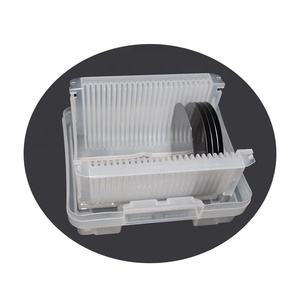
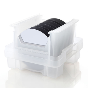
Selection and Procurement on Alibaba.com
Alibaba.com serves as a gateway to a vast selection of n type silicon wafers, connecting buyers with a global network of suppliers. This platform facilitates the discovery of wafers that align with specific electronic project requirements, without the constraints of manufacturing and delivery delays. It's an efficient resource for sourcing these critical components for various industrial and technological applications.